Contact boards and pins
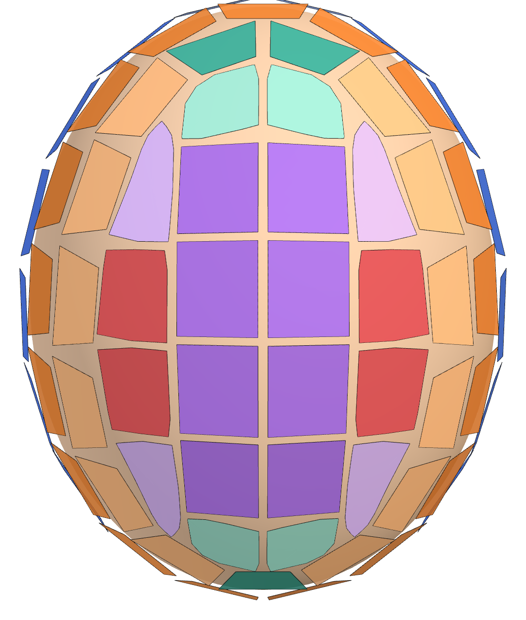
66 flat tiles cover the scalp with 1,118 contacts, and they are only 9 different PCBs: one trapezoid per ring for rings 1-3 (plus a steeper end trapezoid for the front and back of rings 1 and 3) and four shapes for the top. Every design is a real 6-layer, 1.0 mm board: placed, routed and checked, with Gerbers, a BOM and a pick-and-place file for JLCPCB (ordering). There are no controller boards: each tile carries its own converters.
uv run python -m exo.cap_layout                          # the layout          -> out/cap_layout.json (+ .png)
uv run python -m exo.pcb.cap_tiles                       # circuits, placement -> out/pcb/cap/placement.json, boards.json
cd pcb && for d in R1 R1E R2 R3 R3E TA TB TC TD; do ROUTE_OFF=1 PCB_OUT=../out/pcb/cap node tile.mjs $d; done
PCB_OUT=out/pcb/cap uv run python -m exo.pcb.route_all   # Freerouting + repair, every design, in parallel
PCB_OUT=out/pcb/cap uv run python -m exo.pcb.fab_poly    # checks, Gerbers zip, BOM, CPL per design; bom-helmet.csv
PCB_OUT=out/pcb/cap uv run python -m exo.pcb.panel       # the two JLC panels (half a helmet each, assembled twice)
| design | where | tiles | contacts each | outline (mm) | pin gap spread |
|---|---|---|---|---|---|
| R1 | ring 1 (the cuff) | 12 | 20 | trapezoid 29.5 / 26.8 × 21.3 | 1.08 |
| R1E | ring 1, front and back | 2 | 18 | trapezoid 29.7 / 22.4 × 22.1 | 1.31 |
| R2 | ring 2 | 17 | 17 | trapezoid 28.8 / 22.0 × 20.5 | 1.10 |
| R3 | ring 3 | 12 | 17 | trapezoid 29.5 / 21.3 × 20.4 | 1.16 |
| R3E | ring 3, front and back | 3 | 15 | trapezoid 28.2 / 16.4 × 20.8 | 1.21 |
| TA | top, the end cells of the middle strip | 4 | 10 | 9-sided, 20.9 × 24.2 | 0.71 |
| TB | top, the middle double strip | 8 | 18 | 8-sided (a rectangle with trimmed corners), 25.6 × 21.6 | 0.98 |
| TC | top, the ends of the side rows | 4 | 13 | 10-sided, 34.0 × 19.0 | 0.82 |
| TD | top, the middle of the side rows | 4 | 17 | 9-sided, 23.8 × 24.7 | 0.74 |
One pin
Every contact is the same off-the-shelf part, placed by JLC like any other SMD part: the Kinghelm KH-205580-DZ (JLC C530677), an 8.0 mm gold-plated brass pogo pin with a Ø2.0 mm base and a rounded Ø0.9 mm plunger, ~2.0 mm of travel and at most 70 g. It is reflowed onto a Ø2.2 mm pad. The tile's scalp face is set so the pins work between 6.2 mm (0.2 mm short of the plunger bottoming) and 7.7 mm (0.3 mm of preload) from the scalp; on every tile every contact sits inside that, 6.29–7.61 mm in the layout. That one rule sets the size of the tiles: the largest pin-gap spread on any tile is 1.31 mm against the 1.5 mm the pin allows.
How the layout is made (exo/cap_layout.py)
- Rings. A distance field from the cuff line (Dijkstra on a θ/φ grid of the headform) gives level curves parallel to the cuff. Each ring is a band five pin rows high (24.4 mm) between two levels, divided at equal arc length into facets ~32 mm wide; each facet's top corners are the nearest points on the next level up. A ring's trapezoid is the largest that fits nearly all of its facets less the 0.8 mm gap; facets where the ring bends hardest (front and back) get a steeper end trapezoid. Boards on the cuff line or into the hub's space are dropped.
- The top. Above ring 3 the head is nearly flat: the opening is mapped to the plane (azimuthal equidistant, true distances from its centre), made symmetric left-right and under a half turn, and cut by territory lines: a middle double strip of six cells, a fanned row of four cells along each side, an end cell at each corner. Each cell less half the gap is a board; edge cells are trimmed to their own mirror line, so one PCB serves a cell and its mirror twin (a PCB can't be flipped over). The middle strip is stretched 4.5 % and centred so both its ends sit ~1.2 mm from ring 3.
- One PCB per design. Each design's outline is the outline common to every copy (copies aligned to keep it as large as possible), its pins laid out once on a 5.3 mm hexagonal or square lattice inset 2.4 mm from every edge, and its axes turned so the lattice runs along x. Each tile is that design placed by a rigid pose. A design one or two contacts over a multiple of ten drops them (the ones nearest its edge): they would need a converter of their own, and TA, the smallest board, has no room for one. TA has 10 contacts instead of the 12 its outline holds; the helmet 1,118.
Checks (exo.cap_layout fails the build otherwise): every board ≥ 0.8 mm from every other in 3D (0.82 mm worst),
every pin ≥ 2.4 mm from its board's edge in the board's own plane (2.40), every pin gap inside 6.2–7.7 mm, every board
above the cuff and clear of the hub.
On each tile
| per contact | per tile | |
|---|---|---|
| pogo pin on a Ø2.2 mm pad | 1 | |
| 2 × 100k protection, next to the pin | 2 | |
| 220 nF coupling, 10M bias to VMID | 2 | |
| TLV333, gain 101: 100k feedback, 1k to REF_AC | 3 | |
| 1 nF C0G hold capacitor at the converter input | 1 | |
| 47 pF C0G from the amplifier input (AIN) to ground, the input shunt (EMI simulation) | 1 | |
| 100 nF per four amplifiers | ||
| CH32V203G6U6, 12-bit SAR, 10 inputs, its decoupling, BOOT0 pull-down, SWD and reset test pads (scalp face) | 2 | |
| reference: 220 nF + 10M high-pass, the REF filter (10k + 1 nF C0G, 16 kHz) and a TLV333 follower (REF_AC); VMID = 100k/100k + 1 µF | 1 set | |
| two TPS7A2033 LDOs (analog, digital), 4.7 µF in and out | 1 set | |
| SN74LVC1G17 for CLK and SYNC to the next tile, 33R each; 74LVC1G157 closing the UART ring | 1 set | |
| two 12-way 0.5 mm FPC (HC-FPC-05-10-12RLTAG): IN and OUT | 2 | |
| 2 × M2 holes to the shell's standoffs | 2 |
The scalp face carries only the pins, their protection resistors and the test pads; everything else is on the outer face. Every ground and supply pad reaches its plane through a via in the pad, and a through via comes out on the other face: with the scalp face open between the pins those vias always have somewhere to land, and the placer keeps a site clear on the far face for each one. (Putting the front ends beside the pins evened out the faces but left half the plane pads with nowhere for their vias, and the boards did not route.)
Every contact sees two 100k resistors before any silicon, so a fault anywhere on a tile can drive at most
3.6 V / 200 kΩ = 18 µA into the scalp: the highest rail one fault can put on a front end is the port's 3.6 V VIN,
through an LDO failed short (3.3 V / 200 kΩ = 16.5 µA with the LDOs intact). The limit is 50 µA. exo.pcb.fab_poly walks every contact to its first semiconductor and fails
the build if that is ever less. The walk goes through resistors at their value. A capacitor's single fault is a short:
the walk takes each capacitor in turn as 0 Ω, with the others open, and keeps the worst case. So the 220 nF coupling
capacitor is no barrier, and the check measures the 200 kΩ in front of it. A contact that reaches no silicon even with
a capacitor shorted is wired to no front end, and fails. On a cap tile the contacts are the pogo pins: its REF_IN is
the hub's REF follower output, and the reference contact is the hub's, behind its own 200 kΩ (exo.pcb.hub_check).
uv run python -m unittest exo.pcb.test_check holds the rule to a contact with one 100k missing.
The front end. The amplifier's (+) input is the contact, AC-coupled (220 nF, 10M to VMID: 2.2 s, 0.07 Hz); its gain resistor returns to REF_AC, the reference contact coupled and buffered the same way, so the stage amplifies the contact minus the reference by 101 and passes their common part at gain 1. Electrode offsets never see the gain. The input range is ±16 mV around VMID; the TLV333's 350 kHz gain-bandwidth gives ~3.5 kHz closed-loop bandwidth, which is the anti-alias filter ahead of the oversampled converter, and the noise gain of 101 keeps it stable driving the 1 nF hold capacitor directly.
The values come from the EEG simulation, which replays real EEG and synthetic infills through a model of this chain with dry-contact impedances. Its finding: the bias resistor, not the converter, limits a dry-contact front end. Against contacts of hundreds of kΩ to MΩ, 2.2M divides the signal down (to 0.69 at the median contact) and mains up. In the simulation's sweep 10M gains 1.2 dB of alpha SNR at the median contact (1.9 dB at the 10th percentile) and cuts mains at the input from 401 to 108 µV, with almost no clipping (0.03 % of contacts); 22M gains only 0.2 dB more but its bias current (70 pA typical across 22M) clipped 5 % of contacts. The simulation preferred 22M with 100 nF and named 10M as the fallback if the parts' bias current runs high; 10M is the one that keeps margin. At gain 201 mains and offsets used up to 80 % of the range at the 95th-percentile contact; at 101 the SNR changes by under 0.3 dB and the range has room. 220 nF keeps the 2.2 s time constant, and recovers faster from a re-contact step than the old 1 µF/2.2M. VMID is half the analog rail, which is also the converter's reference, so supply noise is ratiometric. TLV333: 55 nV/√Hz, no 1/f corner (zero drift), 100 fA/√Hz current noise (100 nV/√Hz across a 1 MΩ dry contact, under the contact's own 129 nV/√Hz thermal noise).
The converter. One 12-bit LSB at 3.3 V over a gain of 101 is 8.0 µV at the contact. Each CH32V203 scans its ten inputs continuously (TIM1 counting the hub's 2.048 MHz CLK on ETR, PA12, starts the conversions; SYNC on PA15 aligns every converter on the helmet) and averages 64 conversions per channel to each 500 SPS sample (320 kSPS per converter): quantization and the converter's own noise fall by 8, and in the simulation the converter adds about 3 % of the noise power. 12 bits are worth keeping: a 10-bit converter cost 1–5 dB. The firmware trims each microcontroller's internal oscillator against CLK, so the UART runs within its tolerance without a crystal.
Contact impedance
Each converter measures its ten contacts once a second from the hub's contact-quality tone, while the helmet records. The app colours the head map by it while the helmet goes on (the feedback for tightening the ratchet just enough) and uses it to correct each channel's gain. Simulated and host-tested only: no board exists.
How the tone reaches a converter. RP2350 A drives GPIO 46 as a 0/3.3 V square wave, high for the first half period
after every SYNC edge, through 1M/1k into the DRL set point (3.30 mVpp; hub). The DRL holds REF at the set
point through its closed loop L = 1 / (1 + j f / 408 Hz). At the tone the body is one node, so every contact and REF
carry the same tone V_ref. Contact k's (+) node gets H_k V_ref and REF_AC gets H_r V_ref, with the input dividers of
the EEG simulation (sim/hat.py):
H_k = R_b / (R_b + R_prot + Z_e + 1/(jωC))        H_r = R_b / (R_b + 10k + 1/(jωC))
y   = H_amp (G H_k − (G − 1) H_r) V_ref            H_amp = 1 / (1 + j f / 3.47 kHz)   (TLV333 at gain 101)
G H_k and (G − 1) H_r nearly cancel, so the tone at the converter is mostly the contact's own division: y ≈ (1 − G (R_prot + Z_e + 1/(jωC)) / R_b) V_ref. At the median dry contact (900 kΩ ‖ 1 nF) that is about −10 V_ref, 17 LSB at 125 Hz.
The formula the tile computes. With Y the tone's complex amplitude at the converter in LSB (the fundamental, from the one-second I/Q sum, its time origin moved to the SYNC edge by the slot's conversion time 8.5 CLK + s × 2.167 µs):
Z_e = A / (Y + B) − C0,    A = G R_b V,   B = (G − 1) H_r V,   C0 = R_b + R_prot + 1/(jωC)
V   = H_amp(f) L(f) (4/π)(Vpp/2)(−j) e^(−jω t_irq) / LSB        (the expected tone per unit of G H_k − (G − 1) H_r)
It is the divider H_k solved for Z_e. At 125 Hz: A = (−0.825 − 2.375 j) × 10⁹ Ω·LSB, B = −81.5 − 234.9 j LSB,
C0 = 10.2 MΩ − 5.79 kΩ j (firmware/tile/src/imp_tables.h, written by python -m sim.impedance tables). The tile
reports |Z_e| and arg Z_e; the app fits R_e ‖ C_e from them (1/Z_e = 1/R_e + jωC_e) and so has H_k at any frequency.
Check against the simulation (python -m sim.impedance report, out/sim/impedance.json):
- With the nominal parts the inverse returns the contact's own Z_e to 6 × 10⁻¹⁵: it is exactly the model inverted.
- The tile's fixed-point code reproduces sim/impedance.py's integer reference bit for bit (24 vectors). Run on
synthetic conversions of the full model (the square wave's harmonics, scan crosstalk, mains, EEG, drift, noise)
through the simulated ring, the firmware is within 0.3 % + 2 kΩ and 0.2° of the model's fundamental and within 8 %
of the true contact; the difference is the scan crosstalk, which the formula leaves out.
- With part tolerances, 2,000 helmets × contacts (TOL in sim/impedance.py, all assumptions), at 125 Hz:
| p50 | p95 | |
|---|---|---|
| |Z_e| error | 2.5 % | 11 % |
| arg Z_e error | 1.4° | 7.5° |
| R_e fitted | 3.8 % | 19 % |
| |H_k(10 Hz)| for the gain correction | 0.28 % | 1.5 % |
The largest single term is the REF follower's input capacitance (4 pF assumed) against the REF contact and its 200k (12 % p95 alone): it shifts the REF path's phase, and the cancellation above multiplies a relative error between the REF path and a contact path by about 100. Then the PWM amplitude (the 3.3 V rail and the divider, 3.5 %), scan crosstalk (3.1 %), the gain resistors (2.6 %), R_b (2.3 %); noise is 0.7 %.
125 Hz, not 1,024 Hz. 1,024 Hz (2.048 MHz / 2000) would sit outside the EEG band and avoid every mains harmonic. On this front end the analysis prefers 125 Hz (2.048 MHz / 16384):
| 125 Hz | 1,024 Hz | |
|---|---|---|
| DRL closed loop at the tone | 0.956 ∠ −17° | 0.370 ∠ −68° |
| TLV333 closed-loop pole (the anti-alias, 3.47 kHz) | −2.1° | −16.5° |
| resistive share of |Z_e| at the median contact | 0.82 | 0.17 |
| tone at the converter, median contact | 17 LSB | 3.7 LSB |
| one-second SNR, median contact | 52 dB | 45 dB |
| |Z_e| error with tolerances, p50 / p95 | 2.5 % / 11 % | 144 % / 580 % |
| |H_k(10 Hz)| error, p50 / p95 | 0.28 % / 1.5 % | 14 % / 63 % |
| the square wave in the 500 SPS stream | every odd harmonic folds onto 125 Hz (fs/4), −1.3 dB | 24 Hz (−42 dB), 72, 120, 168 Hz |
- Loop bandwidth. The DRL's unity gain is 408 Hz. At 1 kHz the body follows the set point at 0.37 with a 68° lag that moves with the loop's parts (±5 % of f_u is ±7 % of |Z_e| p95 alone). The TLV333's pole adds 16° that moves with its GBW. At 125 Hz both are small and well known.
- What the tone sees. A dry contact's R_e C_e corner is near 180 Hz at the median. At 1 kHz its capacitance carries most of the current, so the resistive part, which sets H_k in the EEG band, is 17 % of |Z_e|, and a degree of phase error is a large error in R_e.
- Parasitics. Every capacitance the formula leaves out (REF follower input, pins) grows with f, and the ×100 cancellation magnifies it: 12 % p95 at 125 Hz, 740 % at 1 kHz.
- SNR. Both are limited by the converter's own noise; the stronger tone at 125 Hz gives 7 dB more.
- Mains. 125 Hz is no harmonic of 50 or 60 Hz; the nearest is 120 Hz. The window is exactly one second, so mains at exactly 60 Hz and its harmonics are rejected exactly; a drifting line leaks well under the noise.
- The cost of 125 Hz. While the tone is on, the stored stream carries a 125 Hz line (about 120 µV at the input at the median contact) inside the 80-200 Hz band. All the square wave's harmonics fold onto exactly fs/4, so the app's derived stream removes it with one notch; the raw (gold) stream keeps it. At 1 kHz the averaging decimator would fold the tone to 24 Hz, inside beta, at −42 dB, and the harmonics to more lines.
1,024 Hz stays in the protocol and the firmware (IMPEDANCE tone_div 2000) for a bench comparison.
On the tile (protocol): the I/Q sum costs ~12 % of the core (counted from the instruction count, not measured), the application grew from 9,864 B to 12,604 B of 14,336 and the static RAM from 3,668 B to 4,076 B of 10 KB.
Not yet known, to measure on the bench: the REF follower's input capacitance and the PWM amplitude (a per-helmet calibration on a phantom of known resistors would remove both, and the DRL's f_u, since they are common to every channel); the scan crosstalk (C_ADC is assumed from the STM32F1); whether dry skin is close enough to R ‖ C (a constant-phase element would make the 125 Hz R_e a slight underestimate of the EEG-band one).
Chains
| 12-way FPC | IN (J101) | OUT (J102) |
|---|---|---|
| 1, 2 | VIN (3.6 V from the hub port) | VIN, passed on |
| 3, 5, 7, 11, tabs | GND | GND |
| 4 | REF from the hub | REF, passed on |
| 6, 8 | CLK, SYNC in | CLK, SYNC re-buffered out (33R) |
| 9 | ring return toward the hub (hub RXD) | ring return from the next tile |
| 10 | data from upstream (hub TXD) | data out to the next tile |
| 12 | GND | SENSE: pulled up; a tile plugged in grounds it |
The pinout is the hub port's own, so a chain's first tile plugs straight into a hub port. Inside a tile the data line
runs into the first CH32V203's RX, from its TX to the second's RX, and from the second's TX out of J102. The return line
comes back in on J102 pin 9 and leaves on J101 pin 9 through a 74LVC1G157: when SENSE is high (nothing on J102: the
last tile of its chain) the mux returns this tile's own last TX instead, closing the ring. exo.pcb.fab_poly checks
that J102 pin n meets J101 pin n of the next tile.
The 66 tiles make 16 chains of three to five (exo.pcb.cap_tiles.chains: balanced clusters of neighbouring tiles,
each ordered as a short path from the tile nearest the hub; the longest tile-to-tile link is 59 mm). A chain of five
carries 10 converters × 10 channels × 500 SPS: ~130 kB/s with framing, under half of a 3 Mbaud line, and draws
~55 mA of the port's 129 mA minimum limit (per tile: two CH32V203 at 48 MHz on the internal oscillator, 4.1 mA each by
WCH's table 4-6-1 plus ~1 mA for the converter, 21 × 17 µA of amplifiers, the buffers).
Routing
tscircuit builds each design from its placement (every land pattern given explicitly), Freerouting routes it
(exo/pcb/route.py: top, inner 2, inner 3 and bottom are signal layers, inner 1 a solid ground plane and inner 4 the
analog supply), and exo/pcb/repair.py finishes whatever Freerouting leaves open on a 0.05 mm grid. Rules: 0.09 mm
track and space (JLCPCB's 6-layer minimum), 0.3/0.2 mm vias, copper 0.3 mm from the edge. After routing every pour is
recomputed around the copper and each design is checked on its own: every net one connected piece of copper, nothing
of two nets closer than 0.09 mm, every contact behind 200 kΩ, the chain pinout.
Every design as routed, changed for the filters and checked (2026-11-04,
on gb10-direct: exo.pcb.fab_poly on out/pcb/cap, KiCad 10.0.7's DRC on the exported board):
| design | part | tiles | layers | parts | traces | vias | open nets | KiCad DRC | REF filter | 47 pF shunts | fab_poly: routed, chain, faults (worst) |
|---|---|---|---|---|---|---|---|---|---|---|---|
| R1 | EXO-511 | 12 | 6 | 252 | 4,144 | 483 | 0 | 0 errors | yes | 20 / 20 | pass (18 µA) |
| R1E | EXO-512 | 2 | 6 | 232 | 4,423 | 486 | 0 | 0 errors | yes | 18 / 18 | pass (18 µA) |
| R2 | EXO-513 | 17 | 6 | 222 | 3,963 | 458 | 0 | 0 errors | yes | 17 / 17 | pass (18 µA) |
| R3 | EXO-514 | 12 | 6 | 222 | 4,637 | 451 | 0 | 0 errors | yes | 17 / 17 | pass (18 µA) |
| R3E | EXO-515 | 3 | 6 | 201 | 4,483 | 479 | 0 | 0 errors | yes | 15 / 15 | pass (18 µA) |
| TA | EXO-521 | 4 | 6 | 141 | 2,042 | 276 | 0 | 0 errors | yes | 10 / 10 | pass (18 µA) |
| TB | EXO-522 | 8 | 6 | 232 | 4,672 | 488 | 0 | 0 errors | yes | 18 / 18 | pass (18 µA) |
| TC | EXO-523 | 4 | 6 | 181 | 4,860 | 461 | 0 | 0 errors | yes | 13 / 13 | pass (18 µA) |
| TD | EXO-524 | 4 | 6 | 222 | 4,512 | 513 | 0 | 0 errors | yes | 17 / 17 | pass (18 µA) |
Parts are every placed part, test points and holes included. "0 errors" is no clearance, width, edge, hole or short error and no unconnected item (KiCad files). Every part has an LCSC number: no design needs Global Sourcing.
The EMI filters (an engineering change)
The EMI simulation asks for two filters on every tile: 10k + 1 nF C0G at the REF follower's input
(RRF1, CRF1: UR1's (+) moves from REF_HP to REF_F) and 47 pF C0G from each amplifier input to ground (CF1.., LCSC
C62546; 100 pF on 2 layers). exo/pcb/cap_tiles.py draws them on both stack-ups. The 6-layer tiles were already
routed, so exo/pcb/eco.py put the parts onto the finished copper instead of a new route:
PCB_OUT=out/pcb/cap-eco uv run python -m exo.pcb.eco R1 R1E R2 R3 R3E TA TB TC TD # each design's routed board
- The fab rules first. The repair runs on the routed board with its copper held (
REPAIR_HOLD=1): tracks too narrow are widened to 0.09 mm, tracks and vias within 0.3 mm of the edge or 0.2 mm of a hole come out and are routed again, dead ends and copper islands with no pad go. Nets the router left open get the repair at its full effort; an open digital net that still does not close gets a 0R jumper (exo/pcb/jumpers.py, digital nets only). - The change. The parts and nets
cap_tilesdraws that the board lacks. Copper of REF_HP that touches UR1's (+) pad is cut, with its dead ends. - The sites. Each part goes in free space next to the pad it joins (UR1 pin 1, or the amplifier's (+) input), on either face. Its courtyard must be clear and its pads 0.09 mm from other nets' copper. Each pad must be able to reach its net around the held copper (a grid of the free cells, the layers joined where a via fits). A ground pad prefers a site for a via in it, and an analog pad prefers 1 mm from clock and UART copper.
- The repair, held.
exo.pcb.repairroutes only what the change opened; no other copper moves. A part whose net it cannot join gets another site (three rounds). Then, once, the repair without the hold may move other nets' traces (the release), and it is undone if it leaves more open. - The checks. pads_check, the board's DRC and
exo.pcb.fab_poly(routed, chain, faults), then KiCad's DRC on the exported board: it passes with no clearance, width, edge, hole or short error.
Result (2026-11-04, on gb10-direct; the routing round's best copy of each design):
| design | REF filter | 47 pF shunts | open nets: router / now | what else moved |
|---|---|---|---|---|
| R1 | yes | 20 / 20 | 1 / 0 | CC14 placed again (no route reached its AIN13 pad) |
| R1E | yes | 18 / 18 | 0 / 0 | |
| R2 | yes | 17 / 17 | 0 / 0 | |
| R3 | yes | 17 / 17 | 3 / 0 | CF5, RH5, CC9, RM1 placed again |
| R3E | yes | 15 / 15 | 0 / 0 | |
| TA | yes | 10 / 10 | 0 / 0 | |
| TB | yes | 18 / 18 | 3 / 0 | |
| TC | yes | 13 / 13 | 1 / 0 | |
| TD | yes | 17 / 17 | 6 / 0 | RG2, RF9 placed again |
Every design: KiCad DRC no error and no unconnected item, every contact behind 200 kΩ (18 µA at 3.6 V), no jumper
needed. 1,118 shunts and 66 REF filters per helmet; the order is $2,107.22 against $2,098.65 without them
(ordering). The 1 mm clock/UART keep-out (the alternative to the shunt) is met by 46 of the 145 design
contacts on the copper as it is, so the shunts are needed. <design>/eco.json in the ECO folder records each part's
site, the nets touched, the segments cut and the open nets in each round.
KiCad files
Every board is also a KiCad 8 project, written from its routed circuit.json, so KiCad and CommandAGI's schematic
and PCB editors open it: pcb/kicad/<board>/<board>.kicad_pcb, .kicad_sch and .kicad_pro for the nine tile
designs, hub (EXO-430) and camera (EXO-450). Rerun the export after routing:
uv run python -m exo.pcb.kicad_export                    # every board -> pcb/kicad/, and pcb/kicad/export.json
uv run python -m exo.pcb.kicad_export R2 hub --check     # some boards, then KiCad's own DRC and ERC on them
- The board is the routed copper as it is: each footprint with its pads where
circuit.jsonputs them, every track and via on its layer with its net, each pour as a zone (its outline is the pour's outer ring, its fill is the pour, stored as KiCad stores a fill: one outline per island, the holes joined by zero-width bridges), the outline on Edge.Cuts, the mounting holes and the stack-up. A via's net is not in the tiles' or the hub'scircuit.json; the export takes it from the copper it touches. The camera's +3V3 tracks and inner-2 fill name a net id that is not in itscircuit.json(the router's+3V3; tscircuit wrote the net asP3V3), and get their net the same way. Vias that are twice incircuit.jsonat one place are written once. - The schematic is a net-label sheet: a box symbol per part, a pin per pad number, a global label of the pin's net
on each pin, and a no-connect flag on each pin of no net. A pad of no net is on KiCad's own net for it
(
unconnected-(J1-Pad1)), as KiCad's update from the schematic names it, so the schematic-parity check passes. - Each part's engineering data is KiCad properties, the forms CommandAGI reads:
CommandAGI IPN(the part's bom.csv line),Manufacturer(from out/sourcing/bom.json),MPN, and one offer,<supplier> Part(the LCSC part) and<supplier> Terms(currency, bom.csv's unit price as the one price, stock, url, source, date). Test points and bare mounting holes are excluded from the BOM. The parts of every board, each board as many times as one helmet has it, give bom.csv's quantity on each of its board lines (export.jsonbom.csv, 2026-11-05: the boards give 114 lines); the one board line they do not give is the camera module (L115), which plugs into the camera board. - KiCad 10.0.7's DRC (with the schematic-parity check) finds no parity problem on any board. On the nine tiles,
as routed and changed (2026-11-04, the filters), it finds no error at
all: no clearance, width, edge, hole or short error and no unconnected item. Its warnings are courtyard overlaps,
slivers, dangling tracks and holes near holes. On the routing round's copper it had found pours 0.187-0.1995 mm from
other-net copper (pours cut with polygons of circles), copper closer than 0.3 mm to the edge on 7 designs and
tracks necked to 0.054-0.0674 mm on R2, R3 and TC. The generators now prevent all three (
exo/pcb/route.pyPOUR_MARGIN andfab_faults,exo/pcb/repair.pyfab_clean). On the hub's first export: J20's four USB-C shield pins (GND, plated) inside the inner-2 VSYS pour with no clearance cut, and 69 vias that touch no copper (fixed in bd1ae13). On the camera's first export: 499 clearance errors, all of them a track or via 0.1875-0.2 mm from a GND or +3V3 pour (KiCad stops counting one kind at 499). The camera's own top and inner-2 fills were cut without POUR_MARGIN;exo/pcb/camera_route.pynow adds it. Re-run 2026-11-05 on the current copper of all eleven boards (the hub with its silkscreen marks, the camera after its pour fix and a repair round): 0 errors on every board, no unconnected item and no parity problem. export.json has every count. - Silkscreen. Every project makes KiCad's silkscreen rules errors, set to JLCPCB's legend rules: text ≥ 1.0 mm
high, line ≥ 0.15 mm, ink ≥ 0.15 mm from copper (
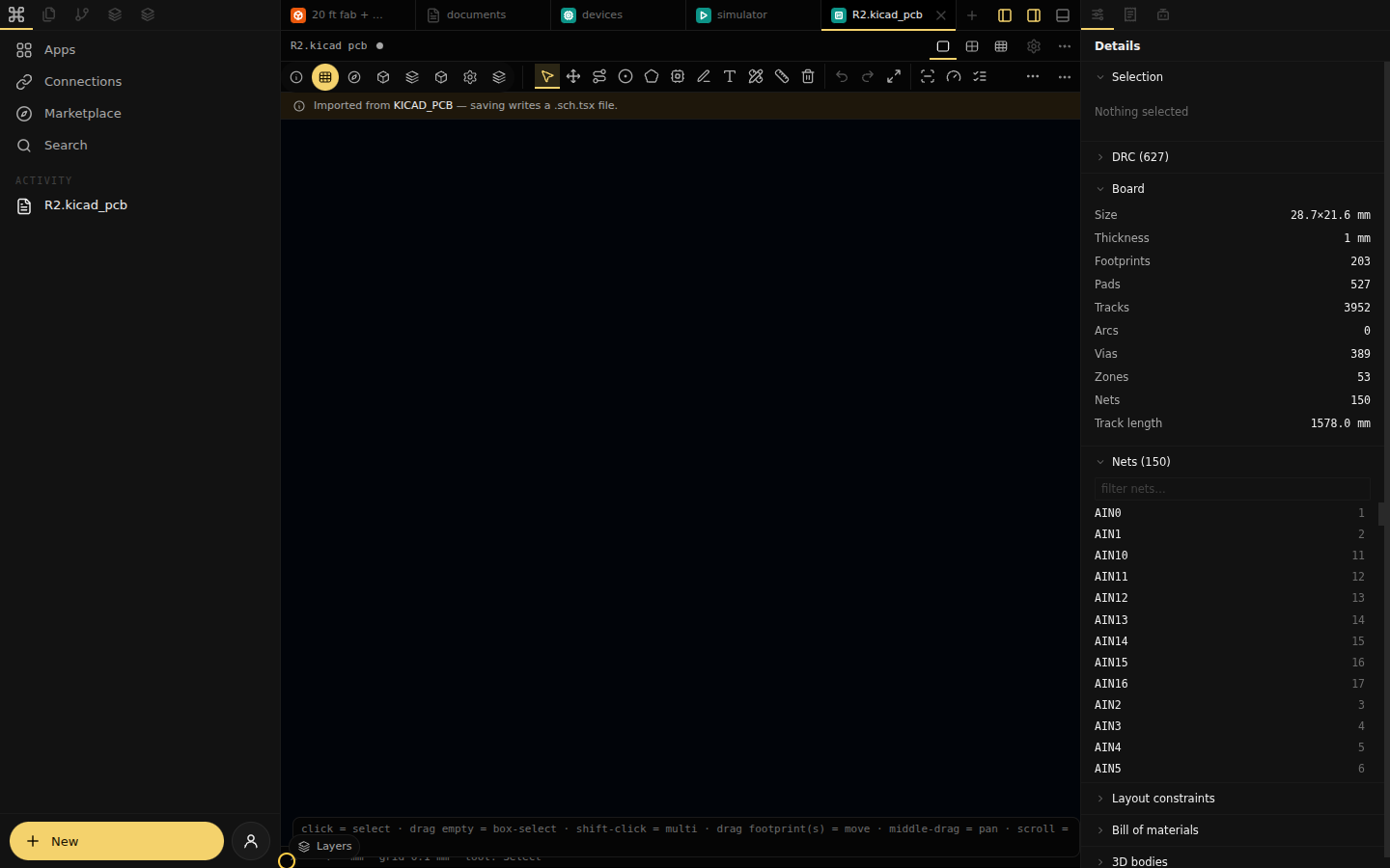
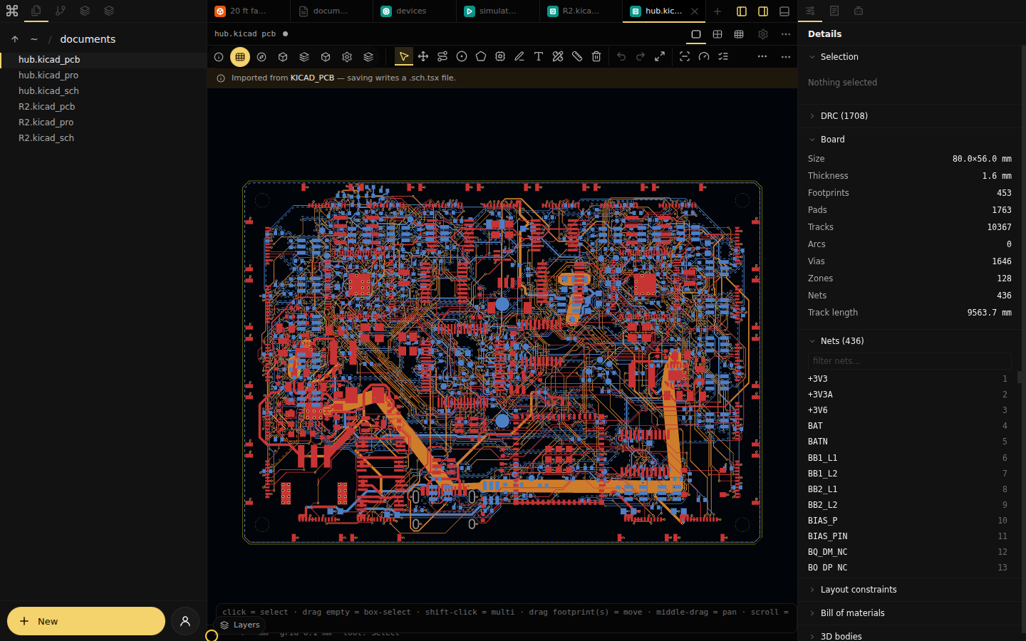
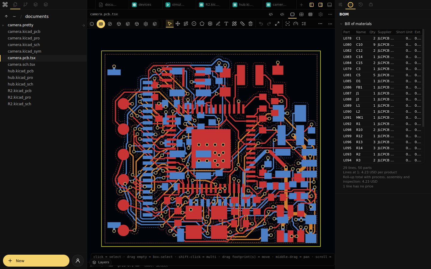
silk_over_copper) and the edge, no silk over silk. The export also runsexo.pcb.silk.silk_faultson each board'scircuit.json, the geometry the Gerbers are drawn from (export.jsonsilk_faults). 2026-11-05: no fault and no silkscreen error on any of the eleven boards. The nine tiles, the two panels and the camera print no silkscreen; the hub prints its marks and its part labels (hub § order files). - In CommandAGI (a workbench of CommandAGI main 567bc5e, 2026-11-04): R2, the hub and the camera board open in the
PCB editor as KiCad imports and draw every footprint, pad, track, via and zone on their layers (R2: 203 footprints,
3,952 tracks, 389 vias, 53 zones on 6 copper layers; hub: 453, 10,367, 1,646, 128 on 4; camera: 55, 1,332, 139, 37
on 4). The board's Bill of materials lists each part with its IPN, maker and MPN. CommandAGI's own reader of the
properties (
logisticsOfFields) gives every part of every board the offer of its bom.csv line: supplier, LCSC part and unit price. The BOM tab needs a cost check, which only the circuit in code declares: Save writes the camera board as code (camera.pcb.tsx, 407 kB), and with<check kind="cost" />added its BOM tab gives 4.2273 USD a board, the sum of bom.csv's prices of its parts. Save refuses R2 (its board in code is over the code sandbox's 1,000,000-byte limit) and the hub (the written schematic does not run to the same circuit), so on the tiles and the hub the BOM tab is not reached; the Bill of materials is.
Two layers and 0R jumpers (a trial)
L2=1 PCB_OUT=out/pcb/cap-l2 LAYOUT=0 SHELL_BUILD=0 bash scripts/cap_pipeline.sh builds the same nine designs as
2-layer boards. There is no plane. Both faces are signal layers. Ground is a fill on both faces, joined by stitching
vias on a 1.5 mm grid and by each ground pad's dogbone via; ground pads that get no dogbone are routed like any net.
The power nets (VIN, +3V3A, +3V3D) are routed as traces and then widened, segment by segment, to the widest of
0.5 / 0.4 / 0.3 / 0.25 / 0.2 / 0.15 mm that keeps the clearance. JLCPCB's rules for 1-2 layers
(capabilities, read 2026-11-03): 0.10 / 0.10 mm track and space;
vias 0.45 mm on a 0.3 mm hole, the quote page's default (a 0.2 mm hole adds plugged vias, a 4-wire Kelvin test and a
via fee: $57 more on the larger panel); no via in pad on 2 layers, so only exposed pads (2 mm and over) take vias, left
open as usual.
Without a ground plane under the front end the tiles pick up more (EMI simulation: unfiltered, median
noise 33 µV, alpha SNR −1.7 dB, 4.4 % of contacts clip; run of 2026-11-03 on 1,118 contacts). The 2-layer build carries the same two filters as the 6-layer
tiles, with 100 pF C0G rather than 47 pF from every amplifier input (AIN) to ground (CF1.., LCSC C62550), and the
10k + 1 nF filter at the REF follower's input (RRF1, CRF1). With them the simulation matches the filtered 6-layer stack (3.66 µV, 19.2 dB with the hub's 8 REF pins and the
contact-potential drift in the budget; 5.27 µV and 16.1 dB with one REF pin). It
expects DC shifts up to 114 µV, a 23 µV spike once a second and up to 3.2 µV of 60 Hz room pickup to remain. Its layout
rules are handled so: the two 100k resistors are placed side by side; digital nets (clock, sync, UART, SWD, the
converters' spare pins) keep 1 mm from the high-impedance analog nets (PIN, PRT, BIN, AIN, FB, REF_IN/HP/F) on the same
face, a class-to-class clearance in Freerouting and in the repair's grid; 2 mm on the other face, each input node's
length (3 mm at most) and the ground under it (2 mm beyond it on the other face) are measured and reported in
route.json's emi; jumpers bridge digital nets only.
Where the routing stays open after Freerouting and the repair, exo/pcb/jumpers.py adds 0R jumpers: the owner's
"overhead wires", but placed and soldered by JLC. A jumper is a 0R chip resistor with both pads on one face; its body
bridges the copper between them. For each piece of a net cut off from the rest, the step looks for a spot where one pad
lands on (or within 0.6 mm of) that piece and the other on the rest of the net, both pads clear of other nets' copper
and the body clear of every other part's courtyard, smallest package first. The jumper goes into placement.json like
any part (both pads on the one net, "jumper": true), so the build, the BOM, the pick-and-place file and the checks
carry it; the router and the checks count its two pads as one conductor. The board is rebuilt and repaired, and the
step repeats until it is clean or no spot is free. What is left is counted as hand wires, pad to pad, in
<design>/jumpers.json.
| jumper | LCSC | part | JLC library |
|---|---|---|---|
| 0402, 1.02 mm between pad centres | C17168 | UNI-ROYAL 0402WGF0000TCE | basic |
| 0603, 1.65 mm | C21189 | UNI-ROYAL 0603WAF0000T5E | basic |
| 0805, 1.83 mm | C17477 | UNI-ROYAL 0805W8F0000T5E | basic |
| 1206, 2.93 mm | C17888 | UNI-ROYAL 1206W4F0000T5E | basic |
Result (2026-11-03, out/pcb/cap-l2 on the peer): the tiles do not route on 2 layers, and jumpers do not change
that. Freerouting leaves about half of each board's connections unrouted (TA 127 of 254) and stops improving
after 10-30 passes. Every board ends with 53-101 nets open. The repair on the grid barely moves it (TA 54
→ 53). Jumpers bridge digital nets only (the EMI rule), and on these boards a jumper's pads displace traces that then
do not reroute: of 13 jumper rounds, 4 closed 1-4 nets and were kept, 9 left more nets open and were undone. Without
the 1 mm digital/analog rule TA still has 47 open nets after Freerouting (54 with it): the cause is the layer count,
not the rule. R2's Freerouting collapses after its first pass every run; its first pass is used.
| design | tiles | layers | open nets | jumpers kept | hand wires (open pieces) | per helmet |
|---|---|---|---|---|---|---|
| R1 | 12 | 2 | 101 | 8 (5 × 0402, 3 × 0603) | 172 | 2,064 |
| R1E | 2 | 2 | 95 | 0 | 162 | 324 |
| R2 | 17 | 2 | 92 | 0 | 162 | 2,754 |
| R3 | 12 | 2 | 90 | 8 (0402) | 160 | 1,920 |
| R3E | 3 | 2 | 85 | 13 (0402) | 160 | 480 |
| TA | 4 | 2 | 53 | 0 | 96 | 384 |
| TB | 8 | 2 | 96 | 0 | 159 | 1,272 |
| TC | 4 | 2 | 78 | 0 | 140 | 560 |
| TD | 4 | 2 | 90 | 14 (11 × 0402, 3 × 0603) | 159 | 636 |
That is 289 jumpers and about 10,400 hand wires per helmet. The EMI layout rules are not met either (route.json
emi): 29-71 digital/analog net pairs closer than 1 mm on a face per board, input-node traces up to 6-38 mm against
3 mm, and a median of 12-26 % of the 2 mm zone around an input node with ground on the other face.
Price, for comparison only: the two panels' bare boards are $73.50 at 2 layers (JLC's quote) against $189.21 in the
6-layer model and $290.58 in JLC's 6-layer quote (0.2 mm vias, epoxy-filled, Kelvin test; fees.json
quotes_2026_11_03). With assembly and the added parts (PCB_OUT=out/pcb/cap-l2 uv run python -m exo.cost) the
order is $1,978.44 against $2,077.84: $99 less on the model, about $200 less on JLC's quotes, before any hand wire.
The other checks pass on every design: pads (no two nets' pads closer than 0.10 mm), no clearance error or short in the routed copper, the chain pinout, and the fault check: with the 220 nF counted as a short (its single fault) every scalp contact of both stack-ups has 200 kΩ before silicon, 18 µA at 3.6 V (2026-11-03; 3.6 V since 2026-11-04).